TSMC Turns to Japanese Substrate Makers as AI's Next Bottleneck Shifts to Light
Taiwan Semiconductor Manufacturing Company (TSMC) is looking to Japan's substrate makers to help address its next major bottleneck: getting light, not just electricity, in and out of AI chips.
Taiwan Semiconductor Manufacturing Company (TSMC) is looking to Japan's substrate makers to help address its next major bottleneck: getting light, not just electricity, in and out of AI chips.
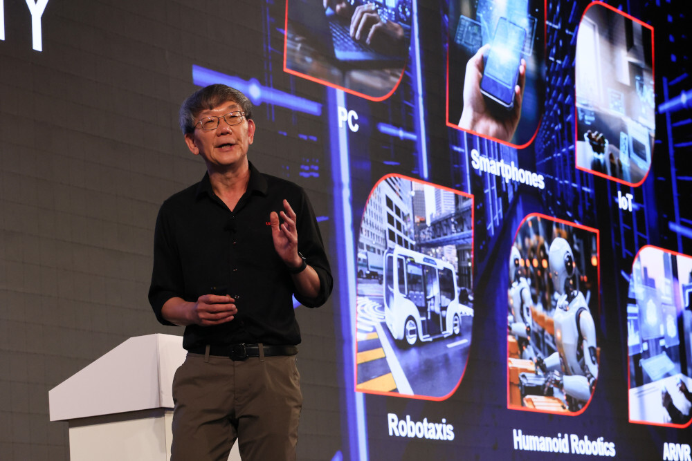
Kevin Zhang, TSMC's senior vice-president and deputy co-chief operating officer, told reporters at the TSMC Technology Symposium in Yokohama on 3 July 2026 that the company is "working very closely with Japanese substrate makers, exploring future substrate technology together." He described Japan as a leader in substrate development.
The technology in question is co-packaged optics (CPO), seen as the next frontier for AI chip packaging. TSMC has not named which companies it is working with, or disclosed any contract — what is confirmed is a stage of collaboration and exploration. This piece looks at what that means for how much value Japan's substrate and optical-component makers can capture as the technology moves towards volume production.
This kind of optoelectronic integration replaces the electrical signals that have long carried data between chips and equipment with light, and co-packaged optics is the approach that brings that conversion right next to the compute chip. As generative AI drives computing demand higher, and data-centre power consumption and heat become harder to manage, the technology is edging towards practical deployment as one answer to that pressure.
What TSMC said
At the centre of the news is TSMC's acknowledgement that Japanese substrate technology could play an important role in this next stage.
Zhang told the Yokohama press briefing that TSMC and Japanese substrate makers are jointly exploring future substrate technology, and positioned Japan as a leading partner. The substrates in question are IC substrates, which carry chips and connect them to external wiring, and interposers, which relay fine circuitry between chip and substrate.
TSMC did not identify specific companies. The description was one of ongoing collaboration and exploration — not a newly announced contract or joint-development deal with a named partner.
Even so, the remark carries weight. TSMC, which dominates contract manufacturing for the world's most advanced chips, has signalled that it regards Japanese technology as important to the substrate foundation for next-generation optical packaging. Which Japanese companies are involved, and in what capacity, is the question to watch next.
Why co-packaged optics, and why now
The pressure behind this shift is the surge in computing and data movement driven by generative AI.
AI training and inference require vast numbers of chips to be linked at high speed, moving huge volumes of data continuously. That data travels across a hierarchy of distances — from links close to the chip to connections across a board, between boards and between racks — and it is the longer links where copper wiring is running out of road. Signal quality degrades sharply as copper runs lengthen, and available bandwidth is approaching a physical ceiling.
Power is the other constraint. Electrical signals lose energy as they travel, consuming more power and generating more heat the longer the distance. In AI data centres, the power needed simply to move signals has become a significant burden in its own right, on top of the power used for computation.
Co-packaged optics moves the point where electricity converts to light as close as possible to the compute chip or switch itself. Optical links can carry data over longer distances with lower transmission loss, power consumption and heat than copper electrical links. Industry estimates suggest that, under comparable conditions, replacing electrical links with optical ones can cut power consumption per unit of bandwidth to a fraction of what copper requires — one reason the sector is racing to develop the technology as a way of managing data-centre power. The closer that conversion point moves to the chip, the more the precision of the substrate and packaging beneath it matters.
What TSMC's "COUPE" actually does
TSMC's answer to this shift is a packaging technology it calls COUPE — the Compact Universal Photonic Engine.
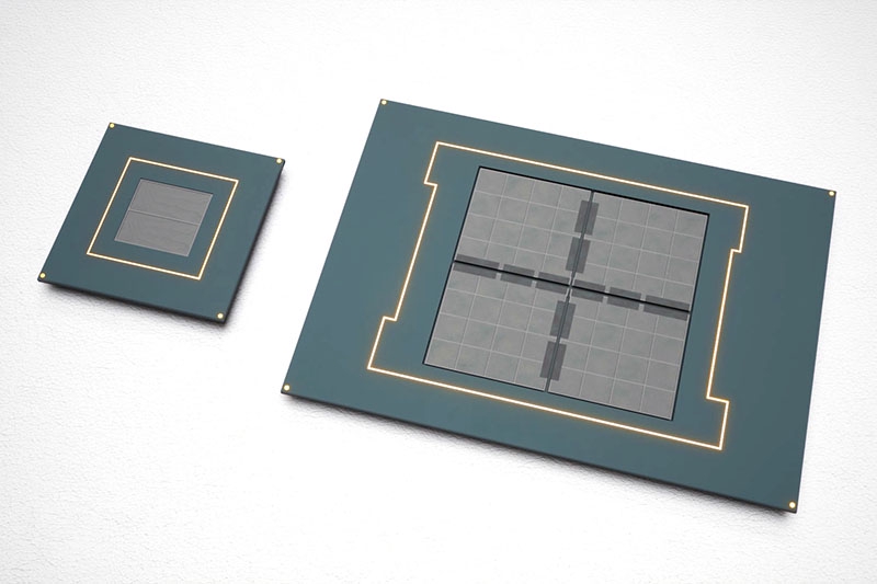
Chips are fundamentally electronic circuits. Co-packaged optics adds a photonic circuit — built in silicon using a technique known as silicon photonics — capable of emitting, receiving and modulating light. COUPE stacks the photonic chip and the electronic chip together and places them immediately next to the compute chip or switch, so the conversion between electricity and light happens over the shortest possible distance. This is the origin of the term "co-packaged optics": the optics and the compute silicon share the same package.
Under TSMC's stated plan, an optical engine incorporating a modulator — which switches the intensity of light at high speed to encode data — and running at roughly 200 gigabits per second per channel, is due to enter volume production in 2026. By 2030, TSMC is targeting a bandwidth density of 4 terabits per second per millimetre of chip edge, to be reached through faster modulators, the simultaneous use of multiple light wavelengths, and multi-row fibre arrays. Both figures are TSMC's own targets, not confirmed outcomes.
CPO is being pursued by several of the largest chipmakers in parallel, and 2026 is regarded in the industry as a potential starting point for a broader ramp-up in volume production.
Where Japan's suppliers stand
Japanese companies hold strength in two distinct layers of this technology. The companies named below are established players in the relevant markets — none has been confirmed as a partner in the collaboration TSMC described.
The first layer is the substrate itself. In the highest-density tier of packaging substrates used for high-performance processors, Ibiden and Shinko Electric Industries between them are estimated to account for the large majority of the global market, with Japanese companies also maintaining a substantial presence in the materials and equipment used to make such substrates. TSMC's description of Japan as a substrate-technology leader reflects this structure.
The second layer is optical connectivity. Co-packaged optics requires extremely precise alignment between photonic circuits and optical fibre, along with specialised connectors for lasers kept outside the package. Sumitomo Electric Industries, Fujikura and Senko Advance are among the established suppliers with strength in this area. Sumitomo Electric, Fujikura and Furukawa Electric have long-standing positions in optical fibre and are positioning themselves to serve rising CPO-related demand.
That position is not unassailable. In the mid-tier of packaging substrates, Taiwanese and South Korean suppliers compete directly with Japanese makers, and a shift towards glass substrates — a newer approach — could erode the advantage Japanese firms have built around conventional plastic-based substrates. In optical components, standardisation of connection methods could make it harder to differentiate on hardware alone. Japan's edge holds most clearly at the leading edge, where precision and yield are hardest to achieve.
Whether it stops at "supplying parts"
What matters for Japanese suppliers is how much value they can capture across the supply chain as this technology scales.
In TSMC's model, TSMC itself integrates the photonic circuit, electronic circuit, substrate and assembly into a single package — and COUPE is the technology that performs that integration. In that structure, Japan's substrate and optical-component makers risk being positioned primarily as suppliers of parts built to TSMC's specification.
Being a supplier is not, on its own, a weak position. A maker of components that cannot easily be substituted retains pricing power and margin. What determines the outcome is a set of more specific questions: how extensively Japanese suppliers can participate in the package-design process; who bears the capital cost of specialised CPO manufacturing equipment; who owns the intellectual property generated along the way; whether suppliers are held responsible for — and rewarded for — production yield; and whether they remain qualified suppliers that are difficult to replace.
Co-packaged optics is a technology where substrates, photonics, assembly and testing are tightly interdependent. Beyond the performance of individual components, what will determine how much value Japanese suppliers capture is the process knowledge needed to manufacture at scale with good yield, and how far they can move into design work spanning both optical and electrical domains. The competitive question is shifting from selling components outright to how deeply suppliers can embed themselves in TSMC's integrated manufacturing process.
What to watch next
What is confirmed so far is TSMC's statement that it is collaborating with Japanese substrate makers to explore future substrate technology, and its COUPE production roadmap. Three things are worth watching from here.
First, which specific Japanese companies TSMC works with, and in what capacity — no names have been disclosed, and the details will likely emerge through future announcements or capital spending by individual suppliers.
Second, whether CPO production scales on schedule. Managing yield and assembly complexity at volume remains an open challenge.
Third, whether Japanese suppliers move beyond parts supply into design and process-integration work. Co-packaged optics is one of a small number of leading-edge fields where Japan's accumulated strength in substrates and optical components is directly relevant — but whether that strength stays confined to meeting someone else's specifications, or extends into shaping design and production decisions, will determine how much of the payoff Japanese companies actually capture. That question sits at the centre of the wider contest over who controls the infrastructure underpinning AI computing — a contest also relevant to the semiconductor supply chains taking shape elsewhere in Asia, including India.