Sony–TSMC Sensor Venture: Kumamoto Expands Beyond Logic Chips Into Image Sensors
Taiwan Semiconductor Manufacturing Co. (TSMC) is set to make Kumamoto a mass-production site not only for logic chips but for image sensors. On 11 August 2026 the foundry signed a definitive agreement with Sony Semiconductor Solutions (SSS) to form an image-sensor joint venture…
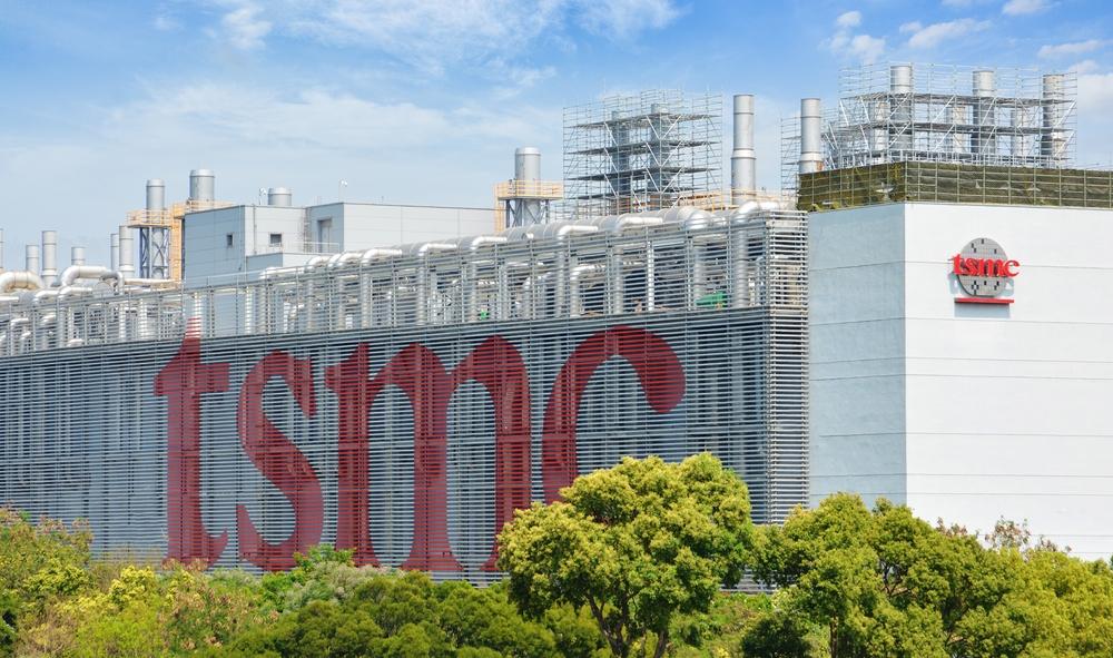
Taiwan Semiconductor Manufacturing Co. (TSMC) is set to make Kumamoto a mass-production site not only for logic chips but for image sensors. On 11 August 2026 the foundry signed a definitive agreement with Sony Semiconductor Solutions (SSS) to form an image-sensor joint venture with combined investment of about ¥747 billion (around US$5.0 billion), with mass production planned for 2029.
TSMC's Japan strategy is moving beyond geographical diversification towards a broader technology base that links design, advanced packaging and volume production to global customers. The question that follows is how deep Japan's materials and equipment makers can get inside that structure.
In brief
- SSS and TSMC signed a definitive agreement on 11 August 2026 to establish a joint venture, "Advanced Vision Semiconductor Manufacturing" (AVSM), to develop and make next-generation image sensors. Of the roughly ¥747 billion (around US$5.0 billion) in combined investment, SSS puts in about ¥465 billion (around US$3.1 billion) to hold control, and TSMC contributes about ¥282 billion (around US$1.9 billion). The site is in Koshi, Kumamoto Prefecture, with mass production planned for 2029.
- In Kumamoto, the first fab of TSMC's logic-production subsidiary JASM (in Kikuyo) began mass production at the end of 2024, and a second fab is due on line in 2027. The planned image-sensor operation would add a second, separate line, giving TSMC two production streams in the prefecture once it starts in 2029.
- TSMC Japan president Makoto Onodera frames Japan as "a base that supports global customers". The company set up a design centre in 2020 and an advanced-packaging R&D centre in Tsukuba in 2021, and the number of Japanese firms it works with there has grown from about 40 to about 120.
- TSMC expects the world semiconductor market to pass US$1 trillion in 2026 and reach around US$1.5 trillion by 2030, with AI and high-performance computing (HPC) making up 55%. That demand is driving advanced packages to grow larger — widening the opening for Japan's substrate and component makers.
Planned sensor venture would give Kumamoto a second production stream
TSMC's Japan strategy has moved beyond contract logic manufacturing alone.
On 11 August 2026, SSS and TSMC signed a definitive agreement to form AVSM, a venture to develop and manufacture next-generation image sensors. Of the roughly ¥747 billion (around US$5.0 billion) in combined investment, SSS provides about ¥465 billion (around US$3.1 billion) and takes management control, while TSMC contributes about ¥282 billion (around US$1.9 billion). SSS will run the venture as a consolidated subsidiary, leading development of the core sensor technology along with product planning and design; TSMC supplies its advanced process technology and manufacturing know-how. The production base sits in Koshi, Kumamoto Prefecture, where the venture plans to begin volume output of next-generation smartphone image sensors in 2029.
An image sensor is the chip that converts the light gathered by a lens into an electrical signal — the part that strongly shapes a smartphone camera's image quality. SSS leads this field worldwide, but South Korea's Samsung Electronics has been gaining share and winning orders from Apple. The venture is best read as a move to lock in advanced production capacity ahead of that competition.
The tie-up did not come from nowhere. The two companies formed a strategic partnership in next-generation image sensors in May 2026, and moved from there to a binding deal in three months. SSS says it will pursue the required investment on the assumption that it receives support from the Japanese government.
Logic in Kikuyo, sensors in Koshi
Kumamoto is already a TSMC logic-production hub; what distinguishes this deal is a second, different manufacturing stream layered on top.
TSMC's production subsidiary JASM (Japan Advanced Semiconductor Manufacturing), backed by investment from SSS and Japan's Denso, sits in Kikuyo, Kumamoto Prefecture. Its first fab entered mass production at the end of 2024, making logic chips at the 22/28-nanometre and 12/16-nanometre generations, with capacity of 55,000 wafers a month on a 300-millimetre-wafer basis. A second fab — which Toyota also joined as an investor — will handle nodes down to the more advanced 6-nanometre generation and is due on line in 2027. Combined capacity across the two fabs is expected to exceed 100,000 wafers a month.
The new venture sits apart from the Kikuyo site, at a facility to be built in Koshi. Within Kumamoto, then, production splits by field: advanced logic at JASM (Kikuyo) and image sensors — a different class of chip that turns light into electrical signals — at AVSM (Koshi). For TSMC, Kumamoto is changing character, from a single-product alternate site into a base that spans several fields.
Opening design, research and fabs to global customers
Onodera casts this build-out as part of a plan to make Japan "a base that supports global customers".
TSMC opened a design centre in Japan in 2020 and, in 2021, established the "TSMC Japan 3DIC R&D Centre" in Tsukuba. The design centre does not serve only Japanese customers; it works with the Taiwan head office and other regional sites to help bring large chips for overseas companies to market. The Kumamoto fabs are, in principle, available to global customers too — a model in which, as Onodera puts it, "the fabs in Japan support demand from customers worldwide".
The Tsukuba centre is where TSMC evaluates and develops next-generation advanced-packaging technology alongside Japanese firms. Its roster of partners has grown from about 40 at the outset to about 120 now. Setting up a domestic point of contact and a clean room — so any issue with a material or component can be tested at once — has helped widen that partner base. Advanced chips are entering a phase where performance turns not only on miniaturisation but on the integration technology that bundles several chips into one package, and Japanese firms hold strengths in the substrates and interposers (the intermediate boards that route connections between chips) this requires. That is why TSMC is expanding its research presence in Japan: to secure that step at home.
Onodera adds that the investments in Arizona and Kumamoto did not start from geopolitics; they rest on customer demand and long-term market growth. As customers increasingly want their supply base spread geographically, simply having a site in Japan has itself become part of what customers prefer.
Sony seeks capacity as TSMC broadens its chip portfolio
The Sony venture is best seen as an answer to a business problem on each side.
SSS's aim is to secure production capacity. Image-sensor shipments are forecast to more than double, from 8 billion units in 2025 to over 20 billion by 2035. Smartphones are not the only driver: uses in which machines "see" their surroundings — robots, security, surveillance, digital health — are spreading. In particular, the spread of physical AI (AI that operates in the real world), embedded in robots and the like, is expected to become a fresh source of demand. With a global capacity shortage looming as demand rises, SSS's investment is better viewed as a move to secure advanced production capacity ahead of rivals. On the technology side, access to advanced packaging such as hybrid bonding — directly joining multiple chips through fine electrodes — also matters. Image-sensor manufacturing is migrating from today's mainstream 65-nanometre and 45-nanometre generations to the 28-nanometre generation, so partnering with a company able to handle finer processes carries real weight.
TSMC has its own motive: broadening the classes of chip it makes. Its smartphone-chip revenue in the second quarter of 2026 (April–June) fell 4% year on year, and the share of total revenue slipped to 22%. As smartphones' weight declines and AI demand surges, TSMC has raised its 2026 capital spending to as much as US$64 billion. Directing part of that investment into image sensors — a stream separate from compute logic — means extending its advanced process technology into a new product area and cementing a long-term bond with a major customer in Sony. This is not a retreat from the smartphone market but a widening of the fields it serves.
Can Japan's suppliers move beyond supplying parts?
Expanding volume production in Kumamoto and deepening research in Tsukuba both mean a wider opening for Japan's materials and equipment makers. But how large the reward is depends heavily on how deep that involvement runs.
Onodera notes that Japan's materials and equipment makers are very strong, from advanced technology through to volume production, and that many Japanese firms are chosen in TSMC's annual supplier awards. As AI and HPC demand drives advanced packages to grow larger, Japanese players strong in substrates and interposers will be drawn into more evaluation and development work.
The question is whether that involvement stops at "supplying parts to specification" or reaches into joint development and process design. Integration technology weaves substrate, packaging and inspection tightly together; what governs added value is not the performance of any single component but the process knowledge to make them yield well at volume. Supplying substrates and interposers is a different position — in pricing power and margin — from taking part in the design of the whole package and the setting of production conditions. Within a structure where TSMC holds the reins of the integration process, a supplier confined to component sales is likely to capture only a limited share of the value. Government support, too, has underpinned TSMC's Kumamoto move from the start, but its payoff should be measured not by the number of plants attracted but by the production capacity and process technology that stay in the country.
What will decide the outcome: ramp-up and process control
TSMC's Japanese operations now span three layers — design, advanced-packaging research and volume production. This venture widens Japan's manufacturing base further, but how much of the reward flows to Japanese industry is not yet settled.
The near-term test is the ramp-up of these large investments. JASM's second fab is due on line in 2027 and the Sony venture, AVSM, plans to start mass production in 2029. Bringing both up on schedule and stabilising yields is the first hurdle. The second is whether the partnerships that have grown to about 120 firms in Tsukuba can be deepened from parts supply into joint development and process design. Bound up with this is the problem Onodera himself calls the industry's biggest — power. Meeting performance demands within a power ceiling requires miniaturisation, 3D integration and optical interconnects to advance in parallel, and the substrates and packaging of that 3D integration are precisely where Japanese players compete.
For now, TSMC and SSS hold the initiative, and the benefits for Japan's materials and equipment makers are not yet assured. The central test is whether the sites TSMC is assembling in Japan remain factories serving global customers, or let Japanese industry earn a return from joint development and process expertise. This ¥747 billion (around US$5.0 billion) venture is one measure of where that dividing line will fall.