Design in India, Equipment in Japan: Complementary Strengths Build a Japan–India Semiconductor Ecosystem
In July 2026, Japan and India took a significant step towards semiconductor cooperation. A joint declaration on economic security placed semiconductors among its priority sectors, setting out a framework that reporting has dubbed a "semiconductor corridor." India brings design…
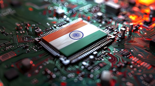
In July 2026, Japan and India took a significant step towards semiconductor cooperation. A joint declaration on economic security placed semiconductors among its priority sectors, setting out a framework that reporting has dubbed a "semiconductor corridor." India brings design and talent; Japan brings manufacturing equipment and materials. Rather than compete, the two are moving to build a semiconductor ecosystem together — starting from back-end processing, design and workforce development. The declaration is a cooperation framework, not a binding investment contract, but for Japan's equipment and materials makers it could open a promising new market.
Key points
- On 3 July 2026, Japan and India signed a Joint Declaration on Economic Security Cooperation, deepening ties across five sectors: semiconductors, critical minerals, information and communications technology (ICT), clean energy and pharmaceuticals.
- On semiconductors, the two agreed to cooperate on manufacturing, research, design and skills development, and welcomed Japanese participation in India's national programme, the India Semiconductor Mission 2.0 (ISM 2.0), and its special economic zones (SEZs).
- The partnership rests on complementary strengths: India's design talent and domestic market, Japan's equipment and materials. Because their strengths do not overlap, the cooperation can be genuinely effective.
- A flagship is the Tata Group's back-end (OSAT — outsourced semiconductor assembly and test) plant at Jagiroad in Assam, planned at about ₹270 billion (roughly US$3 billion) with capacity to assemble and test up to 48 million chips a day.
- More than 100 Japanese semiconductor-ecosystem firms — among them Japan's Tokyo Electron and Sumitomo Chemical — are exploring participation. The near-term focus is back-end processing, design and skills, which could open a new market for equipment and materials suppliers.
What was agreed: manufacturing, research, design and skills
From 1 to 3 July 2026, Prime Minister Narendra Modi hosted Prime Minister Sanae Takaichi in New Delhi for the 16th annual summit between the two countries. The Joint Declaration on Economic Security Cooperation, signed on 3 July, rests on five pillars: semiconductors, critical minerals, ICT, clean energy and pharmaceuticals.
On semiconductors, the two sides agreed to "strengthen and diversify" the supply chains for chip manufacturing. Cooperation spans manufacturing, research, design and skills development, and the declaration welcomed Japanese companies joining India's ISM 2.0 and its SEZs.
It is worth being clear about what the declaration is. It is not an investment contract; it commits no single company to a specific sum or site. It is a government-to-government statement of direction across the five sectors. Even so, by naming concrete areas of cooperation — participation in ISM 2.0, equipment research, workforce development — it goes a step further than the more aspirational agreements of the past. Reporting refers to this set of frameworks as a "semiconductor corridor" or "technology corridor." The division of labour — design in India, equipment and materials in Japan — is a reading of the declaration's cooperation areas, recast as business roles.
Complementary strengths: India in design and market, Japan in equipment and materials
As global semiconductor demand grows and supply chains broaden their base, India's presence is rising quickly. India is estimated to hold about 20% of the world's semiconductor design talent, and its electronics manufacturing is expanding. Through ISM 2.0, the government has widened support beyond attracting fabs to cover manufacturing equipment, materials, domestic IP and full-stack design; in 2025 it raised the semiconductor budget by 83%, to around ₹70 billion. A fast-growing market and design base are drawing chip firms from around the world.
For Japan, India is more than a market. Japan holds a world-class position in manufacturing equipment — lithography, deposition and etching — and in photoresists and ultra-high-purity materials. India has the design talent and the domestic market; Japan has the equipment and materials. Precisely because their strengths are largely complementary, a partnership in which each side fills the other's gaps becomes possible. This complementarity is the single biggest reason the framework could prove effective.
Building the ecosystem from back-end and design
The starting point of this cooperation is not advanced chip fabrication but back-end processing, design and workforce development — and that sequence is a sound way to build an ecosystem.
The flagship project is the Tata Group plant under construction at Jagiroad in Assam. It handles the back-end process known as OSAT (outsourced semiconductor assembly and test), in which semiconductor dies are packaged and tested for defects. The investment is put at about ₹270 billion (roughly US$3 billion), with planned capacity to assemble and test up to 48 million chips a day. Where a front-end fab — which builds the circuits onto the wafer itself — requires investment on the order of trillions of yen and the most advanced tool sets, back-end processing carries a lower barrier to entry and comes on stream faster.
Entering through back-end and design carries real advantages. First, the experience and the workforce for running lines around the clock develop at comparatively low risk. Second, advanced packaging — increasingly important for AI chips — is an extension of back-end work and offers a direct route to more advanced manufacturing. Third, a cluster of back-end activity draws in equipment, materials and design firms, laying the ground for a wider ecosystem that can in time include front-end work. It is a picture of building up steadily, one step at a time, without overreaching.
A new market opening for equipment and materials makers
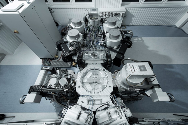
For Japan's equipment and materials makers, this could amount to a promising new market: an expanding Indian semiconductor base generates continuing demand for tools, materials and engineering.
More than 100 Japanese firms across the semiconductor ecosystem are said to be weighing participation — through manufacturing, joint ventures, technology tie-ups, supply-chain localisation and joint research. Named among them are Japan's Tokyo Electron in equipment and Sumitomo Chemical in materials, both reported to be exploring links with Indian partners. For Japan's broad-based semiconductor industry, it could provide a foothold in a growth market.
Turning that opportunity into results, however, will come in stages. The first moves are the most readily actionable: supplying equipment and materials for back-end manufacturing, collaborating on design, and setting up joint-research and skills centres. Local production and large capital projects follow once demand and returns come into view. Separating the stage of selling equipment from the stage of putting down roots makes it possible to deepen the relationship without strain.
The foundations still to be built together: infrastructure and talent
Extending cooperation to advanced front-end work requires foundations that must be built together — which is also where the upside of the partnership lies.
First, infrastructure. A front-end fab needs some two million litres of ultra-pure water a day and near-uninterrupted power. Securing water and power is a decisive condition shaping site selection and investment decisions. Seen in that light, entering first through back-end work — with its less demanding infrastructure requirements — makes sense.
Second, talent. India is rich in design engineers, but its pool of process, equipment and yield engineers — those who keep a front-end line running around the clock — is still developing. Workforce development is written into the cooperation precisely because both sides recognise the gap — and it is an area where Japan's accumulated production know-how can contribute.
Third, time. Standing up an advanced fab takes substantial investment and a long lead time. That is exactly why the chosen sequence — starting with back-end, design and talent and building up in stages — is a realistic and durable path.
What to watch: turning cooperation into substance
The question is whether the framework translates into substance. Three indicators, in order of how soon they should appear. First, whether equipment orders and materials supply for back-end and design work show up as actual sales. Second, whether the interest of more than 100 firms turns into concrete investment in joint ventures and plants. Third, whether infrastructure and talent develop far enough for cooperation to extend into front-end work and advanced packaging.
The three are also a timeline: equipment and materials sales come first, joint ventures and local production follow, and higher-value processes come later.
The Japan–India "semiconductor corridor" is a long-horizon cooperation framework underpinned by a genuine complementarity — design on one side, equipment and materials on the other. Its near-term drivers are back-end processing, design and skills; that is not overreach but a realistic entry point for building an ecosystem steadily. The direction is clear. What remains is whether the two can give the framework substance, one capital investment and one training programme at a time. On semiconductors, Japan and India have taken a first, measured step.